Why we invested in AlixLabs
Semiconductor equipment manufacturer enabling further downscaling of transistors, while improving cost and environmental parameters of its manufacturing.

Scaling semiconductor technology has been an essential to the digitization of society; greatly impacting the way of life, how we consume, communicate and work. For decades, the semiconductor industry has relied on advanced nanostructures and fabrication methods to enable scaling, pushing the limits of engineering and what is doable within the realm of classical physics. Today’s leading edge semiconductor technology requires a complicated, expensive and environmentally burdensome production, orchestrated by a global value chain of design houses, fabrication sites and equipment manufacturers. While this advancement has been driven by end customers’ expectation of continuous advancements in semiconductor technology, the same customers are now to a bigger extent committing to reaching net-zero emissions for their full value chain. Thus, innovation that furthers the leading edge of semiconductor technology while relaxing the resource strain and environmental footprint of the industry, is becoming immensely important.
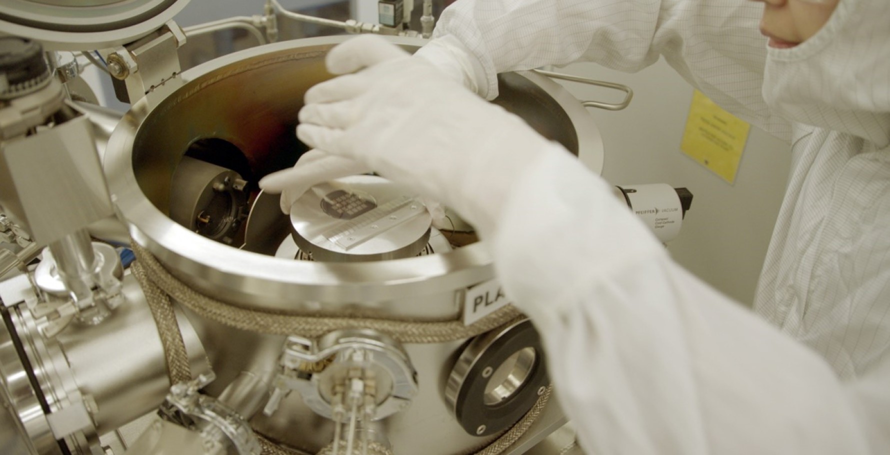
AlixLabs, coming from research at Lund University, is developing fabrication equipment based on a novel method for atomic manipulation of semiconductor structures. The technology has the potential to further the leading edge of transistor manufacturing while enabling cost and resource efficient production of nanometer- (and Ångström)-scaled transistors. With our investment in AlixLabs, we are building an emerging European semiconductor equipment company.

Investment date
January 2023